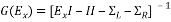
NON EQUILLIBRIUM GREEN’S FUNCTION TECHNIQUE USED FOR THE METAL-INSULATOR-METAL DIODES
ANSHUMAN
Electronics and Communication Dept. NIT Kurukshetra
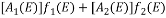
Abstract – In this paper theoretical analysis of NEGF method, including the transport equation and Poisson equation, is done followed by the derivation of an analytical model using NEGF tunnelling probability through any number of insulating layers. Numerical NEGF simulator are shown matching with the AF-TMM simulator results.
THE STUDY OF tunnelling phenomena in Metal Insulator Metal (MIM) is an important topic for the aim of the development of rectennas for energy harvesting and infrared detectors applications. Although the interest in Metal-Insulator-Metal (MIM) diodes dates back to 1950s [1]–[4], but they attracted the attention again in the last few years due to its applications, energy harvesting [5]–[8] and infrared/terahertz detectors [9]–[11].
Earlier, various analytical expressions for the tunnelling transmission probability through MIM diodes were developed based on WKB approximation [2]–[4]. However, the WKB does not take into consideration the wave function reflections at the interface between different layers [14]. Therefore, there came the need for other models to simulate the tunnelling probability. Non Equilibrium Green Function (NEGF) [12] numerical method is one of the methods used to calculate the tunnelling transmission probability [15]–[18]. It is an accurate numerical method, but it needs long time of calculations on a PC in comparison to other analytical models.
Any program used for the simulation of a device performs a solution of transport equation and “Poisson” equation [19].The transport equation gives the electron density, n(r) and the current, I for a known potential profile U(r), while Poisson equation gives the effective U(r), felt by an electron due to the presence of other electron in its vicinity.
Here, in this paper the Quantum transport, Green’s functions and its various equations under non equilibrium condition are discussed and a detailed quantum mechanical modeling of the tunnelling current through MIM diodes is presented. An analytical expression for the tunnelling transmission probability is presented using the NEGF equations for any number of insulator layers between the two metals.


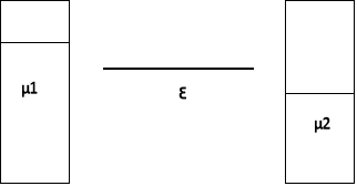


Fig.1. Transport of electrons for single energy level device
The paper is organized as follows: in Section II, the transport equations are discussed. In section III NEGF equations for MIM Diode is described in detail. The governing equations and numerical implementation of it is outlined. The material parameters used in the simulation are also summarized.
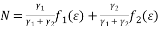
Let’s consider the model for a single device sandwiched between two metals 1and 2ION THE METAL-INSULATOR.ce of other electron in its vicinity.port and “111111111111111111111111111111111111111111, as shown in fig. 1.The device is assumed to be having a single energy level, Ô. Our first aim is to find the number of electrons, N in the device. Let Ef be the Fermi level set by the work function of the two metal contacts under the equilibrium condition. On applying the bias voltage, Vb between metal 1 and 2, the Fermi- energies of two metals gets modified to µ1 and µ2 respectively and given as [19]:
 (1)
(1)
This difference in Fermi-energy gives rise to a non-equilibrium condition and hence two different Fermi-functions for the two contacts. If device is in equilibrium with metal 1, then number of electrons will be f1 but if it is in equilibrium with metal 2, number of electrons will be f2, where
 (2)
(2)
Let  and
and  be the rate of escape of electron from device into metal 1 and metal 2 respectively. Therefore the currents I1 and I2 crossing metal1 and 2 interfaces are given as[20]:
 And
And  (3)
(3)
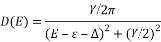
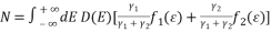
For I1 = I2 = I, we get steady-state number of electrons N and current I as:
 (4a)
(4a)
 (4b)
(4b)
Due to the applied bias voltage one of the reservoir keeps pumping the electron trying to increase the number while the other keeps emptying it trying to lower the number. Ultimately, there is a continuous flow of current, I (eq. 4b) in the external circuit.
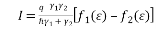
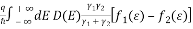
Assuming ðœ‡1 > 𜀠> μ2 and the temperature is low enough that f1 (ε) ≡ f0 (ε − μ1) ≈ 1 and f2 (ε) ≡ f0 (ε − μ2) ≈ 0, the Eq. 4b simplifies to [21]:
 If
If  =
= (5)
(5)
Eq.5 suggests that we can flow an unlimited current through this one level device if we increase , i.e. by coupling the device more and strongly to the metal contacts. But the maximum conductance of a one-level device is equal to
  [20], so there must be some reduction factor.
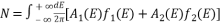
This reduction is due to the broadening of the discrete level that occurs because of increased coupling of the device with the two metals. This broadened discrete level can be described by the distribution:
With line-width of γ and shift of level from ε to ε+∆, where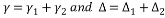 . This broadening phenomena modifies the Eqs. (4a, b) to include an integral over all energies weighted by the distribution D(E) [13]:
 (6a)
(6a)

 (6b)
(6b)
Using algebraic manipulation Eqs. (6a, b) becomes:
 (7a)
(7a)
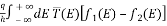 (7b)
(7b)
Where  (8)
(8)
 (9)
(9)
Till now we have discussed device with single energy level ε. But in practical situation (i.e. for real devices) there exist multiple energy levels. Any device, in general, can be represented by a Hamiltonian matrix, whose eigenvalues tells about the allowed energy levels. For example if we describe the device using an effective mass Hamiltonian H =
 then it can be represented with a (NxN) matrix by choosing a discrete lattice with N point and applying methods of finite-differences [13]. This corresponds to using a discretized real space basis.
Similarly, we define self-energy matrices [∑1,2] which describe the broadening and shift of energy levels due to coupling with the two metals. The required NEGF equations now can be obtained from Eqs(7a, b) by replacing scalar quantities ε and σ1,2 with the corresponding matrices [H] and [∑1,2], and is given as:
 ,
,  (10)
(10)
 ,
,  (11)
(11)
The number of electrons N, in the device is replaced with the density matrix, given by:
 {
{ } (12)
Current is still represented by Eq. (7b). The transmission can be given as the trace of the analogous matrix quantity:
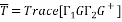 (13)
(13)
The 1D time-independent single-particle Schrödinger equation is given by [13]:
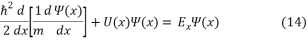
Where,  is the reduced Plank constant, ψ(x) is the electron wave-function, m is the effective mass and U(x) is the potential energy.
If it is assumed that the insulator layers are divided into M grid points having uniform spacing, a, then finite difference discretization on the 1D grid is applied to Schrödinger equation Eq. (1) at each node i as follows [14]:
 (2)
(2)
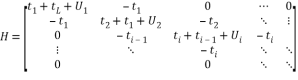
Where , represents the interaction between the nearest neighbour grid points i and i+1, Ui ≡ U (xi), and mi is the electron effective mass between the nodes i and i + 1. The coupling of the potential barrier to the left and right metal electrodes is taken into consideration by rewriting Eq. (1) for i =1 and i = M with open boundary conditions expressed at Metal1/Insulator and Insulator/Metal2 interfaces. So, Schrödinger equation now takes the following form [13]:
 (3)
(3)
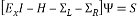
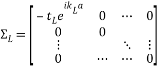
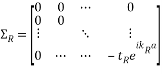
Where, H is the M × M Hamiltonian matrix of the insulator potential, I is the M × M identity matrix, ψ is the wavefunction M × 1 vector and S is M × 1 vector. ∑L and ∑R are the M × M self-energies of the left and right contacts respectively.

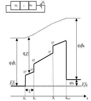
 Fig. 1. Potential of a stack of N insulator materials under applied bias voltage, Vb. Each insulator layer is characterized by a barrier height (Uj), a thickness (d j), a dielectric constant ε j, and an effective mass (m j).
Now, under a tri-diagonal form H can be rewritten as:


∑L and ∑R are given as:


The solution of Eq. (1) can be given in the terms of retarded Green’s function as  where
where  is M×M retarded Green’s function [13]:
The rate of escape of electron to either left or right metal from a given state can be taken into consideration by defining two quantities, ΓL and ΓR [14].
Hence, the tunnelling probability can now be computed as [14]:
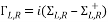
A model of MIIM diode was simulated using NEGF, AF-TMM and WKB Approximation for a comparative analysis of their transmission probability vs. electron transmission energy curve. The parameter spacing, a, for the NEGF calculation was assumed equal to the hundredth of the insulator layer thickness. This was found adequate for reasonable simulation time. The effective mass was assumed equal to the free mass of the electron throughout the MIM structure.
 Fig.3 below shows the
 of the simulated MIIM of Nb/Nb2O5 (2nm)-Ta2O5 (1nm)/Nb at 0.1V of bias voltage. A complete matching between AF-TMM and NEGF results is observed.
|
|
|||||||||
|
|
|||||||||
|
|
|||||||||
|
|
|
|
|
|
|
|
|
|
|

Fig.3. Transmission probability T (Ex) versus the electron transmission energy calculated using AF-TMM, NEGF, and WKB at Vb = 0.1 V for Nb/Nb2O5/Ta2O5/ Nb MIIM diode.
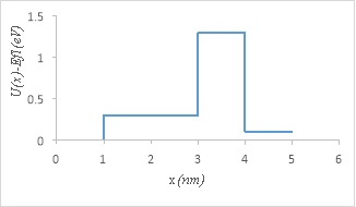
Fig.4. Energy band diagram of the MIIM diode used for simulation
REFERENCES
SYMBOLS
|
Symbol |
Units |
|
|
q |
electronic charge |
1.602 × 10⁻¹⁹ C |
|
H |
Planck constant |
6.626 × 10⁻³⁴ J s |
|
â„ |
h/2π |
1.055 × 10⁻³⁴ J s |
|
M |
free electron mass |
9.11 × 10⁻³¹ kg |
|
ðœº0 |
permittivity of free space |
8.854 × 10⁻¹² F/m |
|
q2/h |
Conductance quantum |
38.7 × 10⁻⁶ S |
|
t0 |
â„ 2/2m*a2 |
electron-volts (eV) |
|
N |
number of electrons or number of photons |
dimensionless |
|
ð†
|
density matrix |
dimensionless |
|
ε
|
energy level |
eV |
|
H
|
Hamiltonian |
eV |
|
U
|
self-consistent potential |
eV |
|
E
|
energy |
eV |
|
μ
|
electrochemical potential |
eV |
|
f(E) |
Fermi function |
dimensionless |
|
D(E)
|
density of states (DOS) |
/eV |
|
A(E) |
spectral function |
/eV |
|
G(E)
|
Green’s function (retarded) |
/eV |
|
|
transmission function |
dimensionless |
|
T (E) |
transmission probability (<1) |
dimensionless |
|
𜸠,ðšª(E)
|
broadening |
eV |
|
ðšº(E) |
self-energy (retarded) |
eV |
Delivering a high-quality product at a reasonable price is not enough anymore.
That’s why we have developed 5 beneficial guarantees that will make your experience with our service enjoyable, easy, and safe.
You have to be 100% sure of the quality of your product to give a money-back guarantee. This describes us perfectly. Make sure that this guarantee is totally transparent.
Read moreEach paper is composed from scratch, according to your instructions. It is then checked by our plagiarism-detection software. There is no gap where plagiarism could squeeze in.
Read moreThanks to our free revisions, there is no way for you to be unsatisfied. We will work on your paper until you are completely happy with the result.
Read moreYour email is safe, as we store it according to international data protection rules. Your bank details are secure, as we use only reliable payment systems.
Read moreBy sending us your money, you buy the service we provide. Check out our terms and conditions if you prefer business talks to be laid out in official language.
Read more


